Index

Hardware Design
The design is fairly minimalist, with few components other than 17 ATmega 328P chips. It consists of:-
• A chassis which holds the backplane and supports the other boards.
• A backplane which interconnects the other components.
• A bus controller. This uses an ATmega 328P to control communication on the bus.
• 16 identical processing nodes. Each one containing an ATmega 328P.

The Chassis
The major parts of this were cut from the back-light diffuser removed from a failed 24 inch computer monitor. The slots, which hold the boards and the backplane, were cut using a small table saw. The material is probably acrylic.
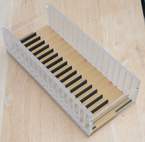
The Backplane
This provides 5-volt power, a common 16MHz clock signal, the data and control signals for inter-processor communication and a common serial input for all the processing nodes. The 5-volt power is derived from the same USB to serial adapter used to connect the system to the computer running the development environment.
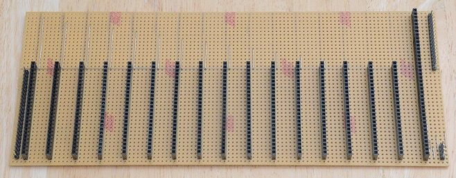
The bus controller requires 40 connections to the bus, however each processing node only requires 25. 16 connections from the bus controller are used to signal that a specific node may use the bus for communication, if it is ready to. These are all fed across the bus to the same connection on each processor node. All of the connections across the back of the board are continuous accept for this one, which is separated between node connectors. This allows all of the processor boards to be identical. Power and serial connections plug into a 4-pin connector at the bottom right of the backplane. A 16-pin connector at the top right and a 25-pin connector at the bottom left allow a logic analyser to be connected for diagnostic purposes.
The Bus Controller
To avoid having to use complicated bus contention hardware, the bus controller has 16 separate connections, via the bus, to each of the processor nodes. It uses these in a cyclic fashion to signal each processing node in turn when it is its turn to use the bus to send data, if it is waiting to do so. If a node is waiting to send data when the bus controller indicates that it can proceed, it has a fixed time window (approximately 20 microseconds) in which to place data and destination information on the bus and to receive an acknowledgement that the communication has been completed if another node is waiting to receive from it. If there is no waiting receiver, the sender remains in a waiting state until there is.
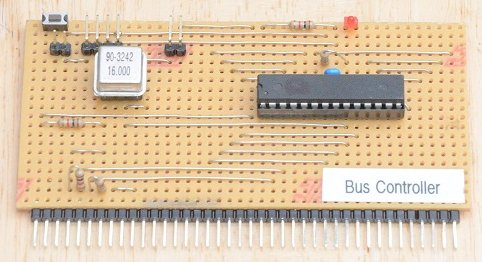
The bus controller board houses the master reset button for the whole system (top left). This resets the bus controller itself and all the processing nodes via the bus. It also houses a 16Mhz clock generator (square package near the reset button). This supplies an external clock for the bus controller itself and for all of the processing nodes via the bus, i.e. the individual 328 chips do not use timing crystals and capacitors in the normal way, nor do they use their own internal clock generators.
The bus controller has its own connector for power and serial connections (right of reset button) allowing it to be programmed independently of the processing nodes. There are 2 links for use during initial configuration. Their use will be described later. A red LED is connected to digital output 13 of the 328 chip in the usual Arduino style. This is useful for testing purposes.
Processing Nodes
The ATmega 328P chips are all loaded with a standard Arduino boot-loader. To allow reliable uploading of programs into all the processing nodes at the same time, each processing node uses the same 16MHz clock source supplied to the bus by the bus controller [1]. In addition, all of the serial receive lines (Rx) on all of the processing nodes are connected together through the bus. One processing node is configured by a link (bottom left, link shown removed) to connect its serial output (Tx) back to the serial connection used to upload software. Thus for programming purposes the whole system behaves like a single processor.
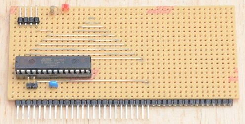
The USB to TTL-level serial adapters used with the multi-processor have 4 wires Rx, Tx, 5 volts and 0 volts. It would be easy to provide an automatic reset function, but this has been omitted here. When uploading programs into the system the master reset button on the bus controller must be pressed when the upload software indicates it is starting the upload. All of the processing nodes receive the same program data via the common Rx connection, and the one nominated by its Tx link sends responses back to the host. All the 328 chips in the system will return identical responses with identical timing due to the common 16MHz clock. In practice, this has turned out to be just as reliable as uploading to a single 328 chip with zero upload failures.
As only one processor node can drive the Tx line back to the host ant any time, an independent, partial serial connection is provided (top left) on each board so that, if required, one or more other nodes could be connected to serial adapters. This connector only supports the Tx and 0 volt connections to the chip.
A red LED is connected to digital output 13 of the 328 chip in the usual Arduino style. This is useful both for testing and for providing a visual activity indicator for a node.
Next: Bus Organisation
~~~~~~~~~~~~~~~~~~~~~~~~~~~~~~~~~
1. It is not necessary to program on-chip fuses specially to use an external clock in this way and default fuse settings were used when burning the boot-loaders into the chips. The clock is connected to the X1 clock inputs of all the chips. This input is internally connected to an inverting gate, called an “inverting amplifier” in the Atmel documentation. The output of the gate connects directly to the chip's internal clock line. Therefore without an external crystal and timing capacitors this gate simple inverts the clock signal supplied. The clock signal is a square wave so this just results in an inverted square wave,