Index

Schematics
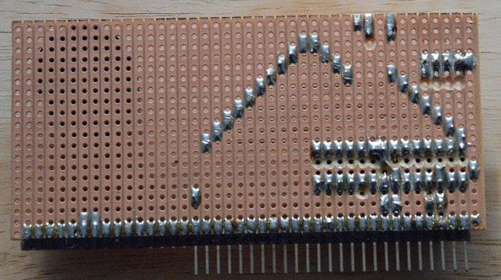
Bus Controller

Click for larger image.
Front and rear views of the bus controller board are shown below. The board shown has an an extra link (top and to the right of the clock module) and an extra pull-up resistor (top and to the left of the LED) which allow the state of the, otherwise unused, A5 pin on the chip to be controlled. These are not shown on the schematics and are not relevant to anything described in this article.
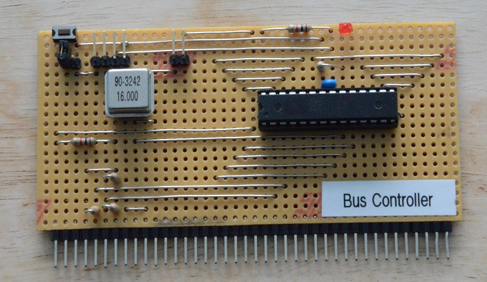
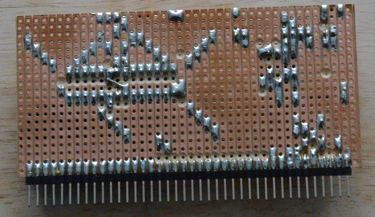
Notice that on the rear of the board there is a diagonal wire link connecting the Vcc pin on one side of the chip to the AVcc and AVref pins on the other. Not visible on the front view of the board is a similar link connecting the two 0v pins, pins 8 and 22. This is hidden under the IC and its socket.
Processing Nodes
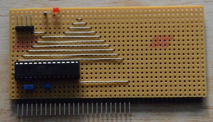
All of the processing node boards are identical.
Click for larger image.
Front and rear views are shown below. Again there is a hidden link between the two 0v pins not visible under the IC and its socket. The board shown has the its serial output link installed (blue rectangle lower left next to the 100nF decoupling capacitor). This can only be installed on one node to allow it to send serial output via the main serial connector. However independent serial outputs can be connected to any of the processing nodes via the output only serial connector at the top left of each board.
The Bus

Click for larger image.
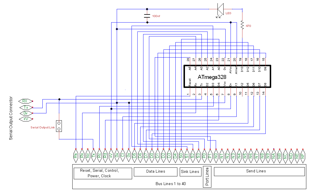
The physical layout of the bus is very much dictated by the position of the pins on the 328 chip and the availability of the various functions assigned to the internal port registers. In particular no single port provides 8 bits for the data bus, and this is split over ports B and D. This also makes it difficult to order the data bus lines from D0 to D7. Instead they are ordered D5, D6, D7, D0, D1, D2, D3 and D4.
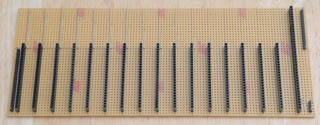
In the above image the bus controller socket is on the right and the common reset line is at the bottom. A 40-pin socket is used for the bus controller as it requires access to lines on both sides of the bus. Individual processor nodes only connect to the first 25 lines on the bus so 25-pin sockets are used. The only other components on the board are the master serial connector for programming the nodes (lower right), 2 diagnostic sockets for connecting a logic analyser (lower left and top right), and a 1k pull-up resistor (hidden behind the bus controller socket) for the common Rx serial line to hold it at 5 volts if the system is run without a serial connection plugged into the main serial connector, e.g. while initially configuring the node identifiers with the system powered via the alternative serial connector on the bus controller board.
Next: Firmware