Index

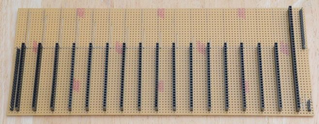
Bus Organisation
The bus carries several different kinds of signal.
• 16 lines which allow the bus controller to indicate which processor node can take control of the bus to attempt a send operation.
• 17 lines which allow communication to take place between processor nodes.
• 7 lines which carry power, the shared 16MHz clock signal and serial Rx and Tx lines.
The 0 volt power rail is duplicated (to provide a partial ground plane for the clock) and one line is not used (because it simplified processor node layout), making 40 lines in all.
The bus controller generates sequences of non-overlapping, negative going pulses on each of the lines connected to the individual processor nodes as shown below. These pules have a duration of approximately 20 microseconds and tell each processing node when it can take control of the bus to attempt to send data to a potential receiver. This is the only way the bus controller is involved in communication. It is not connected to any of the other communication lines on the bus. Generating these bus control pulses could have been achieved using a 4-bit counter and a 4 to 16 line decoder but using another micro-controller to do the job provides greater flexibility, e.g. in controlling the gap between pulses and organising some of the initial configuration of the system.

Figure 2
The following diagram illustrates the timing of send operation involving node 0.
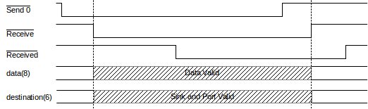
Figure 3
When a node is not in control of the bus all of its pins connected to the bus will be configured as inputs so as not to interfere with other nodes. Assuming that node 0 is waiting to send, nothing happens until the bus controller asserts the send 0 line on the bus. At this point an interrupt routine in the node 0 software (defined by the DataFlow library) will be invoked as a result of the negative edge (pin change interrupt). This routine will set the pins connected to the data lines (8 bits) and the pins connected to the destination lines (4 bits for the node identifier and 2 bits for the port) to outputs and set their values. It will then assert the receive line to tell other nodes that the data is valid.
Any nodes waiting to receive at this point will respond to the negative edge of the receive line with their own interrupt routines. These will input the destination bits and check to see if the specified node identifier corresponds with their own node identifier and if they are waiting to receive on the specified port. If both of these conditions are satisfied, the node concerned will input the data and assert the received line to tell the sender that the communication has been completed.
The sender keep asserting the receive line until it sees the send line from the bus controller go high again. The receiver will continue to assert the received line until it sees the receive line return to a high state (it is not connected to the same send line). If the sender is not waiting to send when the bus controller asserts its send line, it will do nothing. In fact the associated pin change interrupt will not even be enabled. If there are no waiting receivers or none of the waiting receivers match the destination specified by the sender, the received line will not be asserted and the sender will try again the next time the bus controller asserts its send line.
The order of the lines on the bus and their mapping to processor pins is shown below.
| Bus Line | Function | Processor Pin | Comment |
|---|---|---|---|
| 1 | reset | reset | |
| 2 | rx | rx | |
| 3 | - | No Connection | |
| 4 | tx | tx | |
| 5 | receive | D3 | |
| 6 | received | D4 | |
| 7 | +5 volts | +V, Va | |
| 8 | 0 volts | 0 volts | |
| 9 | clock | X1 | |
| 10 | 0 Volts | 0 Volts | |
| 11 | data bit-5 | D5 | |
| 12 | data bit-6 | D6 | |
| 13 | data bit-7 | D7 | |
| 14 | data bit-0 | D8 | |
| 15 | data bit-1 | D9 | |
| 16 | data bit-2 | D10 | |
| 17 | data bit-3 | D11 | |
| 18 | data bit-4 | D12 | |
| 19 | sink bit-0 | A0 | Used as digital pin |
| 20 | sink bit-1 | A1 | " |
| 21 | sink bit-2 | A2 | " |
| 22 | sink bit-3 | A3 | " |
| 23 | port bit-0 | A4 | " |
| 24 | port bit-1 | A5 | " |
| 25 | send | D2 |
Lines 25 to 40 carry the send signals from the bus controller to each of the processor nodes, starting with send 0. However, to avoid each processor node having its send signal on a different pin, these lines are all connected across to line 25 on each processor node socket. This line is separated between the sockets for the individual processor nodes. All the other lines run the entire length of the board.
The discontinuous ordering of the pins used for the data bits is caused by the arrangement of the 328's I/O port registers. There is no contiguous set of 8 bits available in any port register that can be used for digital I/O. Thus the lower 5 bits of port B are used together with the upper 3 bits of port D. The 4 bits required for the destination node identifier (sink 0 to 3) plus the 2 bits required for the destination port, map directly onto the 6 available bits in port C, which are generally used for analogue inputs, but also work as fully functional digital pins.
Next: Library Software